CHEMISTRY THE CENTRAL SCIENCE
12 SOLIDS AND MODERN MATERIALS
12.9 NANOMATERIALS
The prefix nano means 10–9. ![]() (Section 1.4) When people speak of “nanotechnology,” they usually mean making devices that are on the 1–100-nm scale. It turns out that the properties of semiconductors and metals change in this size range. Nanomaterials—materials that have dimensions on the 1-100-nm scale—are under intense investigation in research laboratories around the world, and chemistry plays a central role in this investigation.
(Section 1.4) When people speak of “nanotechnology,” they usually mean making devices that are on the 1–100-nm scale. It turns out that the properties of semiconductors and metals change in this size range. Nanomaterials—materials that have dimensions on the 1-100-nm scale—are under intense investigation in research laboratories around the world, and chemistry plays a central role in this investigation.
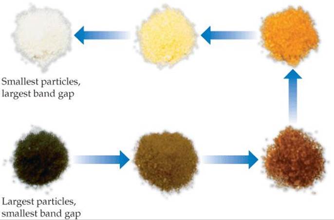
![]() FIGURE 12.43 Cd3P2 powders with different particle sizes. The arrows indicate decreasing particle size and a corresponding increase in the band gap energy.
FIGURE 12.43 Cd3P2 powders with different particle sizes. The arrows indicate decreasing particle size and a corresponding increase in the band gap energy.
Semiconductors on the Nanoscale
Figure 12.23 shows that, in small molecules, electrons occupy discrete molecular orbitals whereas in macroscale solids the electrons occupy delocalized bands. At what point does a molecule get so large that it starts behaving as though it has delocalized bands rather than localized molecular orbitals? For semiconductors, both theory and experiment tell us that the answer is roughly at 1 to 10 nm (about 10-100 atoms across). The exact number depends on the specific semiconductor material. The equations of quantum mechanics that were used for electrons in atoms can be applied to electrons (and holes) in semiconductors to estimate the size where materials undergo a crossover from molecular orbitals to bands. Because these effects become important at 1 to 10 nm, semiconductor particles with diameters in this size range are called quantum dots.
One of the most spectacular effects of reducing the size of a semiconductor crystal is that the band gap changes substantially with size in the 1-10-nm range. As the particle gets smaller, the band gap gets larger, an effect observable by the naked eye, as shown in ![]() FIGURE 12.43. On the macro level, the semiconductor cadmium phosphide looks black because its band gap is small (Eg = 0.5 eV), and it absorbs all wavelengths of visible light. As the crystals are made smaller, the material progressively changes color until it looks white! It looks white because now no visible light is absorbed. The band gap is so large that only high-energy ultraviolet light can excite electrons into the conduction band (Eg > 3.0 eV).
FIGURE 12.43. On the macro level, the semiconductor cadmium phosphide looks black because its band gap is small (Eg = 0.5 eV), and it absorbs all wavelengths of visible light. As the crystals are made smaller, the material progressively changes color until it looks white! It looks white because now no visible light is absorbed. The band gap is so large that only high-energy ultraviolet light can excite electrons into the conduction band (Eg > 3.0 eV).
Making quantum dots is most easily accomplished using chemical reactions in solution. For example, to make CdS, you can mix Cd(NO3)2 and Na2S in water. If you do not do anything else, you will precipitate large crystals of CdS. However, if you first add a negatively charged polymer to the water (such as polyphosphate, —(OPO2)n—), the Cd2+ associates with the polymer, like tiny “meatballs” in the polymer “spaghetti.” When sulfide is added, CdS particles grow, but the polymer keeps them from forming large crystals. A great deal of fine-tuning of reaction conditions is necessary to produce nanocrystals that are of uniform size and shape.
As we learned in Section 12.7 some semiconductor devices can emit light when a voltage is applied. Another way to make semiconductors emit light is to illuminate them with light whose photons have energies larger than the energy of the band gap of the semiconductor. This process is called photoluminescence. A valence-band electron absorbs a photon and is promoted to the conduction band. If the excited electron then falls back down into the hole it left in the valence band, it emits a photon having energy equal to the band gap energy. In the case of quantum dots, the band gap is tunable with the crystal size, and thus all the colors of the rainbow can be obtained from just one material, as shown for CdSe in ![]() FIGURE 12.44.
FIGURE 12.44.
![]() GO FIGURE
GO FIGURE
As the size of the quantum dots decreases, does the wavelength of the emitted light increase or decrease?
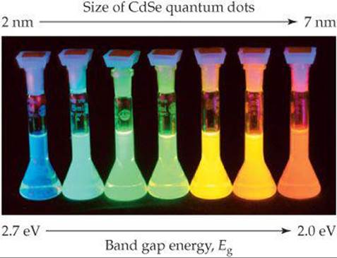
![]() FIGURE 12.44 Photoluminescence. When illuminated with ultraviolet light, these solutions, each containing nanoparticles of the semiconductor CdSe, emit light that corresponds to their respective band gap energies. The light emitted depends on the size of the CdSe nanoparticles.
FIGURE 12.44 Photoluminescence. When illuminated with ultraviolet light, these solutions, each containing nanoparticles of the semiconductor CdSe, emit light that corresponds to their respective band gap energies. The light emitted depends on the size of the CdSe nanoparticles.
![]() GIVE IT SOME THOUGHT
GIVE IT SOME THOUGHT
Large crystals of ZnS can show photoluminescence, emitting ultraviolet photons with energies equal to the band gap energy and a wavelength of 340 nm. Is it possible to shift the luminescence so that the emitted photons are in the visible region of the spectrum by making appropriately sized nanocrystals?
Quantum dots are being explored for applications ranging from electronics to lasers to medical imaging because they are very bright, very stable, and small enough to be taken up by living cells even after being coated with a biocompatible surface layer.
Semiconductors do not have to be shrunk to the nanoscale in all three dimensions in order to show new properties. They can be laid down in relatively large two-dimensional areas on a substrate but be only a few nanometers thick to make quantum wells. Quantum wires, in which the semiconductor wire diameter is only a few nanometers but its length is very long, have also been made by various chemical routes. In both quantum wells and quantum wires, measurements along the nanoscale dimension(s) show quantum behavior, but in the long dimension, the properties seem to be just like those of the bulk material.
Metals on the Nanoscale
Metals also have unusual properties on the 1-100-nm-length scale. Fundamentally, this is because the mean free path ![]() (Section 10.8) of an electron in a metal at room temperature is typically about 1–100 nm. So when the particle size of a metal is 100 nm or less, one might expect unusual effects.
(Section 10.8) of an electron in a metal at room temperature is typically about 1–100 nm. So when the particle size of a metal is 100 nm or less, one might expect unusual effects.
Although it was not fully understood, people have known for hundreds of years that metals are different when they are very finely divided. Dating back to the middle ages, the makers of stained-glass windows knew that gold dispersed in molten glass made the glass a beautiful deep red (![]() FIGURE 12.45). Much later, in 1857, Michael Faraday reported that dispersions of small gold particles could be made stable and were deeply colored—some of the original colloidal solutions that he made are still in the Royal Institution of Great Britain's Faraday Museum in London (
FIGURE 12.45). Much later, in 1857, Michael Faraday reported that dispersions of small gold particles could be made stable and were deeply colored—some of the original colloidal solutions that he made are still in the Royal Institution of Great Britain's Faraday Museum in London (![]() FIGURE 12.46).
FIGURE 12.46).
Other physical and chemical properties of metallic nanoparticles are also different from the properties of the bulk materials. Gold particles less than 20 nm in diameter melt at a far lower temperature than bulk gold, for instance, and when the particles are between 2 and 3 nm in diameter, gold is no longer a “noble,” unreactive metal; in this size range it becomes chemically reactive.
At nanoscale dimensions, silver has properties analogous to those of gold in its beautiful colors, although it is more reactive than gold. Currently, there is great interest in research laboratories around the world in taking advantage of the unusual optical properties of metal nanoparticles for applications in biomedical imaging and chemical detection.

![]() FIGURE 12.45 Stained glass window from the Chartres Cathedral in France. Gold nanoparticles are responsible for the red color in this window, which dates from the 12th century.
FIGURE 12.45 Stained glass window from the Chartres Cathedral in France. Gold nanoparticles are responsible for the red color in this window, which dates from the 12th century.
Fullerenes, Carbon Nanotubes, and Graphene
We have seen that elemental carbon is quite versatile. In its sp3-hybridized solid-state form, it is diamond; in its sp2-hybridized solid-state form, it is graphite. Over the past three decades, scientists have discovered that sp2-hybridized carbon can also form discrete molecules, one-dimensional tubes, and two-dimensional sheets. Each of these forms of carbon shows very interesting properties.
Until the mid-1980s, pure solid carbon was thought to exist in only two forms: the covalent-network solids diamond and graphite. In 1985, however, a group of researchers led by Richard Smalley and Robert Curl of Rice University in Houston and Harry Kroto of the University of Sussex, England, vaporized a sample of graphite with an intense pulse of laser light and used a stream of helium gas to carry the vaporized carbon into a mass spectrometer (Section 2.4, “A Closer Look: The Mass Spectrometer”). The mass spectrum showed peaks corresponding to clusters of carbon atoms, with a particularly strong peak corresponding to molecules composed of 60 carbon atoms, C60.

![]() FIGURE 12.46 The solutions of colloidal gold nanoparticles made by Michael Faraday in the 1850s. These are on display in the Faraday Museum, London.
FIGURE 12.46 The solutions of colloidal gold nanoparticles made by Michael Faraday in the 1850s. These are on display in the Faraday Museum, London.
Because C60 clusters were so preferentially formed, the group proposed a radically different form of carbon, namely, nearly spherical C60molecules. They proposed that the carbon atoms of C60 form a “ball” with 32 faces, 12 of them pentagons and 20 hexagons (![]() FIGURE 12.47), exactly like a soccer ball. The shape of this molecule is reminiscent of the geodesic dome invented by the U.S. engineer and philosopher R. Buckminster Fuller, so C60 was whimsically named “buckminsterfullerene,” or “buckyball” for short. Since the discovery of C60, other related molecules of carbon atoms have been discovered. These molecules are now known as fullerenes.
FIGURE 12.47), exactly like a soccer ball. The shape of this molecule is reminiscent of the geodesic dome invented by the U.S. engineer and philosopher R. Buckminster Fuller, so C60 was whimsically named “buckminsterfullerene,” or “buckyball” for short. Since the discovery of C60, other related molecules of carbon atoms have been discovered. These molecules are now known as fullerenes.
Appreciable amounts of buckyball can be prepared by electrically evaporating graphite in an atmosphere of helium gas. About 14% of the resulting soot consists of C60 and a related molecule, C70, which has a more elongated structure. The carbon-rich gases from which C60 and C70condense also contain other fullerenes, mostly containing more carbon atoms, such as C76 and C84. The smallest possible fullerene, C20, was first detected in 2000. This small, ball-shaped molecule is much more reactive than the larger fullerenes. Because fullerenes are composed of individual molecules, they dissolve in various organic solvents, whereas diamond and graphite do not. This solubility permits fullerenes to be separated from the other components of soot and even from one another. It also allows the study of their reactions in solution.
Soon after the discovery of C60, chemists discovered carbon nanotubes (![]() FIGURE 12.48). You can think of these as sheets of graphite rolled up and capped at one or both ends by half of a C60 molecule. Carbon nanotubes are made in a manner similar to that used to make C60. They can be made in either multiwall or single-walled forms. Multi-wall carbon nanotubes consist of tubes within tubes, nested together, whereas single-walled carbon nanotubes consist of single tubes. Single-walled carbon nanotubes can be 1000 nm long or even longer but are only about 1 nm in diameter. Depending on the diameter of the graphite sheet and how it is rolled up, carbon nanotubes can behave as either semiconductors or metals.
FIGURE 12.48). You can think of these as sheets of graphite rolled up and capped at one or both ends by half of a C60 molecule. Carbon nanotubes are made in a manner similar to that used to make C60. They can be made in either multiwall or single-walled forms. Multi-wall carbon nanotubes consist of tubes within tubes, nested together, whereas single-walled carbon nanotubes consist of single tubes. Single-walled carbon nanotubes can be 1000 nm long or even longer but are only about 1 nm in diameter. Depending on the diameter of the graphite sheet and how it is rolled up, carbon nanotubes can behave as either semiconductors or metals.
The fact that carbon nanotubes can be made either semiconducting or metallic without any doping is unique among solid-state materials, and a great deal of work is going on to make carbon-based electronic devices. Carbon nanotubes are also being explored for their mechanical properties. The carbon-carbon bonded framework of the nanotubes means that the imperfections that might appear in a metal nanowire of similar dimensions are nearly absent. Experiments on individual carbon nanotubes suggest that they are stronger than steel, if steel were the dimensions of a carbon nanotube. Carbon nanotubes have been spun into fibers with polymers, adding great strength and toughness to the composite material.
![]() GO FIGURE
GO FIGURE
How many bonds does each carbon atom in C60 make? Based on this observation would you expect the bonding in C60 to be more like that in diamond or that in graphite?
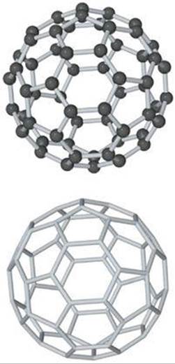
![]() FIGURE 12.47 Buckminsterfullerene, C60. The molecule has a highly symmetric structure in which the 60 carbon atoms sit at the vertices of a truncated icosahedron. The bottom view shows only the bonds between carbon atoms.
FIGURE 12.47 Buckminsterfullerene, C60. The molecule has a highly symmetric structure in which the 60 carbon atoms sit at the vertices of a truncated icosahedron. The bottom view shows only the bonds between carbon atoms.
The two-dimensional form of carbon, graphene, is the most recent low-dimensional form of carbon to be experimentally isolated and studied. Although its properties had been the subject of theoretical predictions for over 60 years, it was not until 2004 that researchers at the University of Manchester in England isolated and identified individual sheets of carbon atoms with the honeycomb structure shown in ![]() FIGURE 12.49. Amazingly, the technique they used to isolate single-layer graphene was to successively peel away thin layers of graphite using an adhesive tape. Individual layers of graphene were then transferred to a silicon wafer having a precisely defined overcoat of SiO2. When a single layer of graphene is left on the wafer, an interference-like contrast pattern results that can be seen with an optical microscope. If not for this simple yet effective way to scan for individual graphene crystals, they would probably still remain undiscovered. Subsequently, it has been shown that graphene can be deposited on clean surfaces of other types of crystals. The scientists who led the effort at the University of Manchester, Andre Geim and Konstantin Novoselov, were awarded the 2010 Nobel prize in physics for their work.
FIGURE 12.49. Amazingly, the technique they used to isolate single-layer graphene was to successively peel away thin layers of graphite using an adhesive tape. Individual layers of graphene were then transferred to a silicon wafer having a precisely defined overcoat of SiO2. When a single layer of graphene is left on the wafer, an interference-like contrast pattern results that can be seen with an optical microscope. If not for this simple yet effective way to scan for individual graphene crystals, they would probably still remain undiscovered. Subsequently, it has been shown that graphene can be deposited on clean surfaces of other types of crystals. The scientists who led the effort at the University of Manchester, Andre Geim and Konstantin Novoselov, were awarded the 2010 Nobel prize in physics for their work.
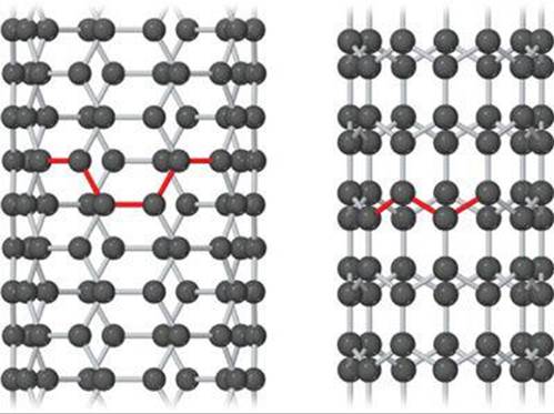
![]() FIGURE 12.48 Atomic models of carbon nanotubes. Left: “Armchair” nanotube, which shows metallic behavior. Right: “Zigzag” nanotube, which can be either semiconducting or metallic, depending on tube diameter.
FIGURE 12.48 Atomic models of carbon nanotubes. Left: “Armchair” nanotube, which shows metallic behavior. Right: “Zigzag” nanotube, which can be either semiconducting or metallic, depending on tube diameter.
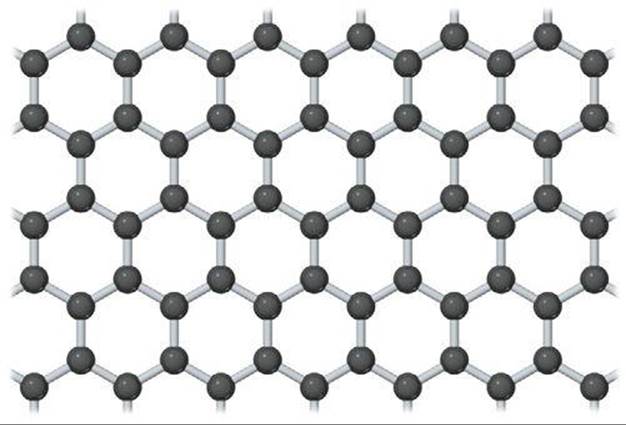
![]() FIGURE 12.49 A portion of a two-dimensional graphene sheet.
FIGURE 12.49 A portion of a two-dimensional graphene sheet.
The properties of graphene are remarkable. It is very strong and has a record thermal conductivity, topping carbon nanotubes in both categories. Graphene is a semimetal, which means its electronic structure is like that of a semiconductor in which the energy gap is exactly zero. The combination of graphene's two-dimensional character and the fact that it is a semimetal allows the electrons to travel very long distances, up to 0.3 μm, without scattering from another electron, atom, or impurity. Graphene can sustain electrical current densities six orders of magnitude higher than those sustainable in copper. Scientists are currently exploring ways to incorporate graphene in various technologies.
SAMPLE INTEGRATIVE EXERCISE Putting Concepts Together
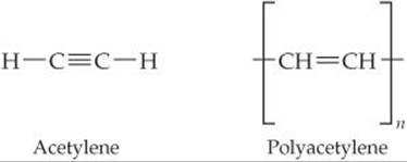
A conducting polymer is a polymer that can conduct electricity. Some polymers can be made semiconducting; others can be nearly metallic. Polyacetylene is an example of a polymer that is a semiconductor. It can also be doped to increase its conductivity.
Polyacetylene is made from acetylene in a reaction that looks simple but is actually tricky to do:
(a) What is the hybridization of the carbon atoms, and the geometry around those atoms, in acetylene and in polyacetylene?
(b) Write a balanced equation to make polyacetylene from acetylene.
(c) Acetylene is a gas at room temperature and pressure (298 K, 1.00 atm). How many grams of polyacetylene can you make from a 5.00-L vessel of acetylene gas at room temperature and room pressure? Assume acetylene behaves ideally, and that the polymerization reaction occurs with 100% yield.
(d) Using the average bond enthalpies in Table 8.4, predict whether the formation of polyacetylene from acetylene is endothermic or exothermic.
SOLUTION
Analyze For part (a), we need to recall what we have learned about sp, sp2, and sp3 hybridization and geometry. ![]() (Section 9.5) For part (b), we need to write a balanced equation. For part (c), we need to use the ideal-gas equation.
(Section 9.5) For part (b), we need to write a balanced equation. For part (c), we need to use the ideal-gas equation. ![]() (Section 10.4) For part (d), we need to recall the definitions of endothermic and exothermic and how bond enthalpies can be used to predict overall reaction enthalpies.
(Section 10.4) For part (d), we need to recall the definitions of endothermic and exothermic and how bond enthalpies can be used to predict overall reaction enthalpies. ![]() (Section 8.8)
(Section 8.8)
Plan For part (a), we should draw out the chemical structures of the reactant and product. For part (b), we need to make sure the equation is properly balanced. For part (c), we need to convert from liters of gas to moles of gas, using the ideal-gas equation (PV = nRT); then we need to convert from moles of acetylene gas to moles of polyacetylene using the answer from part (b); then we can convert to grams of polyacetylene. For part (d), we need to recall that ΔHrxn = Σ (bond enthalpies of bonds broken) — Σ(bond enthalpies of bonds formed).
Solve
(a) Carbon always forms four bonds. Thus, each C atom must have a single bond to H and a triple bond to the other C atom in acetylene. As a result, each C atom has two electron domains and must be sp hybridized. This sp hybridization also means that the H—C—C angles in acetylene are 180° and the molecule is linear.
We can write out the partial structure of polyacetylene as follows:
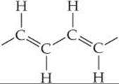
Each carbon is identical but now has three bonding electron domains that surround it. Therefore, the hybridization of each carbon atom is sp2, and each carbon has local trigonal planar geometry with 120° angles.
(b) We can write:
![]()
Note that all atoms originally present in acetylene end up in the polyacetylene product.
(c) We can use the ideal-gas equation as follows:
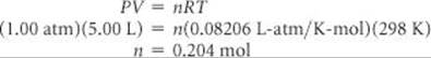
Acetylene has a molar mass of 26.0 g/mol; therefore, the mass of 0.204 mol is
(0.204 mol)(26.0 g/mol) = 5.32 g acetylene
Note that from the answer to part (b), all the atoms in acetylene go into polyacetylene. Due to conservation of mass, then, the mass of polyacetylene produced must also be 5.32 g, if we assume 100% yield.
(d) Let's consider the case for n = 1. We note that the reactant side of the equation in part (b) has one C≡C triple bond and two C—H single bonds. The product side of the equation in part (b) has one C═C double bond, one C—C single bond (to link to the adjacent monomer), and two C—H single bonds. Therefore, we are breaking one C≡C triple bond and are forming one C═C double bond and one C—C single bond. Accordingly, the enthalpy change for polyacetylene formation is:
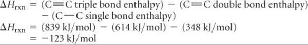
Because ΔH is a negative number, the reaction releases heat and is exothermic.