Microreactors in Organic Chemistry and Catalysis, Second Edition (2013)
2. Fabrication of Microreactors Made from Metals and Ceramic
2.6. Assembling and Bonding of Metal Microstructures
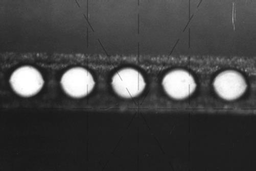
While assembling of a number of device parts is not really a problem in the macroscale world, on microscale this step is more delicate to handle. The main point is the adjustment and alignment accuracy of the parts. Moreover, sealing, fixation, and bonding technology problems may also occur, depending on the material and the process parameters the device is designated for. Depending on the surface quality and the bonding technology applied, aligning errors may reach similar dimensions as the microstructures themselves. An example is shown in Figure 2.11. Here, a number of wet chemically etched microstructure foils have been aligned in a poor way to form elliptically shaped microchannels. Figure 2.12 shows two correctly aligned foils, forming nearly circular microchannels. Misalignment will lead to nonregular channels and therefore may interfere with the bonding technique; in severe cases, it may lead to the destruction of the complete device. A correct alignment will lead to only small deviations from the desired elliptical shape, and the distortion during the bonding process will be small. Alignment techniques used to avoid errors can be simple mechanical methods (e.g., use of alignment pins), edge catches in a specially designed assembling device, or optical methods such as laser alignment. These methods are easily automated, as shown in semiconductor technology. In fact, most of the methods come from silicon processing technology, where precise alignment of multiple mask layers is needed to guarantee the functionality of the manufactured devices [1, 3].
Figure 2.11 Photo of an arrangement of wet chemically etched microchannel foils. Due to misalignment, in some layers the microchannels are not formed correctly to elliptically shaped channels.
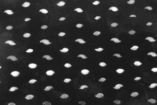
Figure 2.12 Photo of two wet chemically etched foils arranged and aligned correctly to form nearly circular microchannels.
Another problem of the microscale is the surface quality of the single parts of a device. While the mean roughness is not of major concern (see Ref. [11]), burr formation by mechanical micromachining or laser machining may lead to significant problems during assembling of device parts as well as during the bonding process. Thus, special attention has to be paid to burr microstructures or to avoid burr formation. It might even be necessary to apply special techniques such as electropolishing or smoothening to burr the single parts.
Bonding of metals can be done by using numerous techniques. The common techniques used for microstructures are welding (laser, e-beam, others), brazing, diffusion bonding, and low-temperature as well as high-temperature soldering. Even clamping and sometimes, for very specific applications, gluing, including different sealing techniques, can be used. Details of the processes can be found in Refs [1, 2, 4, 5, 22–25], (Pfeifer, P. et al. (2004) Micromotive, unpublished results.) [26–28], (Pfleging, W. and Lambach, H., unpublished results).
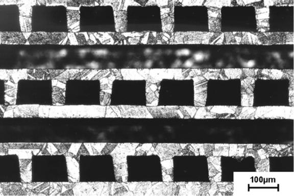
For high-pressure applications and very secure run of chemical reactions, diffusion-bonded metal devices are the optimum choice. Due to the process of diffusion bonding (stacking, applying defined mechanical pressure force to the stack, heating in vacuum or inert atmosphere to about 80% of melting temperature, cooling down while the mechanical pressure force is applied), a more or less monolithic block including microstructures is generated, which is extremely stable at high pressures. Due to the diffusion of material from one foil to another, no borderline limitations between single foils in terms of heat transfer exist anymore. Thus, the thermal behavior of diffusion-bonded devices is superior in comparison to devices manufactured by other bonding techniques. In Figure 2.13, clockwise, the diffusion bonding process chain is shown, starting with the single foils' stack of a cross-flow stainless steel device. Figure 2.14 shows a cut through a diffusion-bonded stainless steel device. Crystal growth across the foil borderlines is clearly seen. However, it is very evident that a technique like this is limited to materials that do not show any chemically different layer on top of the surface. Oxide layers (like those generated on top of aluminum materials) are prohibitive for diffusion bonding. They can be removed by a preliminary reduction step. This of course increases the efforts for bonding drastically, and it is questionable whether a change of material provides more advantages than such a complex bonding.
Figure 2.13 Diffusion bonding process chain. Clockwise, starting top left: stacking, diffusion bonding furnace with mechanical pressure force, diffusion bonding, and cut through a microchannel system after diffusion bonding.
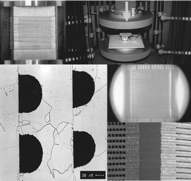
Figure 2.14 Cut through a diffusion-bonded cross-flow arrangement of stainless steel microchannel foils. Clearly, the crystal growth over the borderlines between the single foils is shown. Thus, diffusion bonding led to the formation of a monolithic stainless steel device.
It is obvious that the choice of the bonding technique has to be made depending on the process parameters. It is not possible to run a device bonded by low-temperature soldering at some 100 °C. Thus, the most relevant parameters for the choice of bonding technique are process temperature, process pressure, and corrosivity of the process chemicals.