Microreactors in Organic Chemistry and Catalysis, Second Edition (2013)
3. Microreactors Made of Glass and Silicon
3.2. The Structuring of Glass and Silicon
In microsystems engineering, another process is important besides the structuring of thin layers, which is the etching of the solid material. This will now be described in more detail.
From the point of view of the mechanical characteristics, glass and silicon resemble each other. They have a similar mechanical hardness, are brittle as they lack plasticity, and are thus prone to brittle fracture. Of the standard precision engineering procedures available for shaping, only those that do not use a geometrically defined cutter can be used, such as grinding and lapping. Microengineering techniques are much more efficient but do prove difficult for deeper structures.
3.2.1 Structuring by Means of Masked Etching As in Microsystems Technology
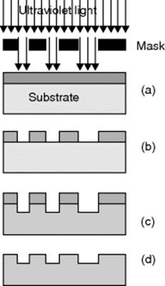
On the whole, microsystems procedures rely on masking, whether the aim is to create the structure by the addition or the subtraction of material. The areas not intended to be affected by the procedure are shielded from it by a protective mask. In the cases described here, through-holes or cavities are produced by subtraction of material. The masking acts as a shield, for instance, against an aggressive etch or the chemical changes associated with the photoresist technique (Figure 3.4). A distinction must be made between the mask for photolithography and the type of masking required for an ensuing process of substance removal. In the case of photolithography, a light pattern is directed onto the surface of the substrate after it has been coated with photosensitive material (photoresist), resulting in resolutions on the micrometer scale. For the required structures, this is sufficiently accurate. The mask, or reticle, used in photolithography is a layer of glass or transparent polymer coated with certain absorber structures. For microelectronics, there are procedures available, which can achieve much higher resolution. See Refs [2–4] for more details.
Figure 3.4 Photolithography: (a)photoresist laid on and exposed with a mask; (b) developing; (c) etched substrate; (d) photoresist removed.
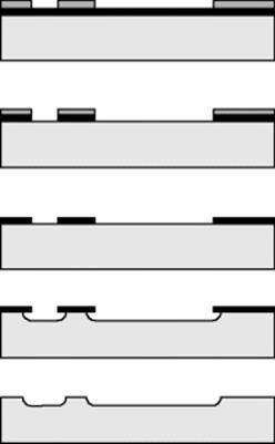
The photochemical processes in photoresist may work as a positive resist, enhancing the solubility of the exposed areas, or as a negative resist, reducing the solubility. At a later stage of the manufacturing process, the easier-to-dissolve portions will be removed. It is possible to use this photoresist mask for certain substance-removal procedures, as in the case of the special resist for microsandblasting, or for plasma etching of silicon. Where this is not usable because not selective enough, two-stage masking is necessary. Such is the case for deep wet chemical etching of glass and for anisotropic etching of silicon. Here, a masking layer of several hundred nanometer thickness is painted onto the substrate; for the structuring of glass, the mask is made of CrNi and polysilicon, and for silicon, it is a single SiO2 Si3N4 layer. This coating is then etched with the aid of the photoresist and a suitable etching medium, Figure 3.5. The selectivity achieved with this combined masking layer is much greater than that with photoresist alone. In addition to photolithography, other, more direct types of lithography are possible.
Figure 3.5 Etching with a second masking layer.
The means of masking will be described together with the structuring processes for which they are used.
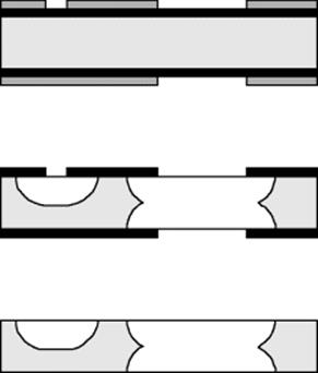
To produce through-holes and cavities in a wafer, special forms of lithography are employed. If it is assumed that a roughly constant amount of material requires to be removed from all over the wafer, the creation in one and the same process of both cavities and holes is not feasible. The only possibility to achieve this is to perform masking and lithography from both sides and then etch both sides simultaneously. The through-holes will be on both sides but the cavities only on one side. The second option is a two-stage lithography. In the first stage, the cavities are made, and then, the wafer is masked again and the holes are created in the second stage (Figure 3.6).
Figure 3.6 Two-stage (double-sided) lithography.
3.2.2 Etching Technologies
Etching processes are the ones that offer the highest geometrical resolution as far as microtechnology is concerned. With it, structures accurate to <1 mm are possible. In contrast to the way machining or “shaving” processes work, etch processes deal with the whole wafer at once, that is, the whole of the surface of one or more wafers is treated simultaneously. The etch rate and selectivity are important parameters.
The types of etch process are divided into wet or dry chemical etching and isotropic or anisotropic etching as shown in Figure 3.7.
Figure 3.7 Isotropic and anisotropic etching.

If the material etched away is removed as a liquid, the term used is wet chemical etching. The term dry chemical etching is used when the material is removed in the gaseous state. Each type can be isotropic, with the same etch rate operating in all directions, or anisotropic, with etch rates reflecting direction, which may be a spatial direction or the crystal orientation.
The materials glass and silicon can be subjected to every combination. To achieve structure sizes required for micoreactors, the following are used:
1. anisotropic (crystallographic) wet chemical etching of silicon (KOH);
2. isotropic wet chemical etching of silicon (HF + HNO3 + CH3COOH + H2O);
3. isotropic dry chemical etching of silicon (reactive ion etching: RIE);
4. isotropic wet chemical etching of glass (buffered 10% hydrofluoric acid);
5. anisotropic dry etching with inductively coupled plasma for silicon and glass, the maximum for glass is 40–50 μm, problem is the small etching rate [5].
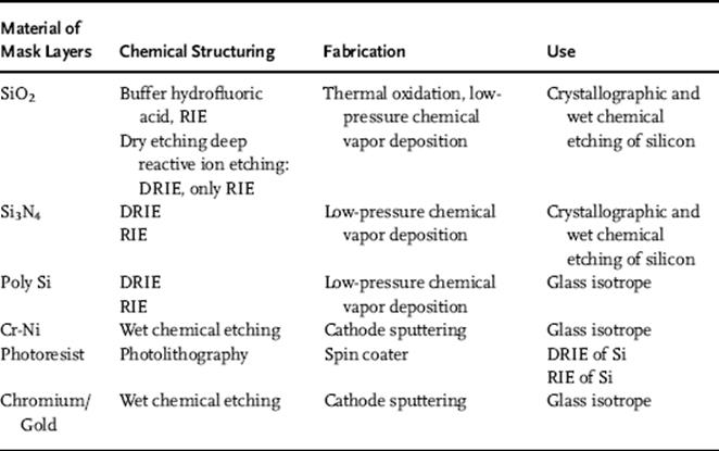
A number of commonly used masking layers are listed in Table 3.3.
Table 3.3 Material of mask layers.
3.2.2.1 Anisotropic (Crystallographic) Wet Chemical Etching of Silicon (KOH)
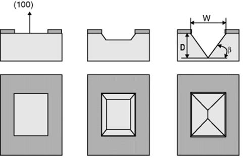
In anisotropic crystallographic wet chemical etching of silicon, the fact that the etch rate depends on the crystal orientation is exploited. Even along the main levels of the crystal, for example, along the (111)- and (110)-level, the etch rate can vary by a factor of 100. Aqueous solutions of the alkali metals such as KOH and NaOH are anisotropic etch solutions for silicon. The speed of etching in the individual directions will depend on the temperature and the etch solution used. The relation of the etch rate to the crystal's direction is shown in Figure 3.8 for the widely produced wafers made of (100)-type silicon [2].
Figure 3.8 Schematic representation of the speed of etching of the lateral direction (100) silicon (50% aq. KOH at 78 °C).
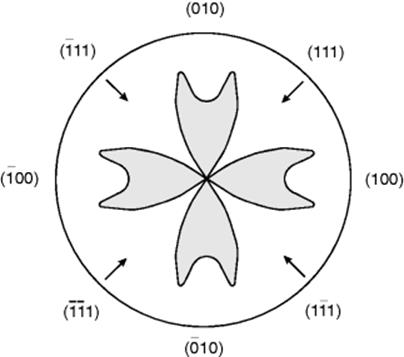
Figure 3.9 show the shapes obtained when silicon is etched anisotropically. The four (111) levels cut the surface of a disc of (100) material along the (110) directions within it. The etchant attacks each layer of the (100) levels in turn and removes them; Figure 3.9 is a diagram of the process. Any push forward on the part of the (100) base is prevented laterally by the (111) levels slowly being etched. Apart from slight undercutting of the mask, the (111) levels seem stable. The angle β to the vertical is 54.75°. At that, the etching effectively ceases. The ratio of the width of the trough (w) to its depth (t) is
![]()
Figure 3.9 Etching until the natural etch stops.
The masking material used is SiO2 or Si3N4 (see Table 3.3). Rectangular mask openings oriented in the (110) direction lead to the creation of rectangular troughs that are limited by the four (111) levels. These have the effect of a natural etch barrier. A square opening means inverted pyramids will form. Openings shaped in any other ways will always produce V-shaped troughs if the etching is continued until the natural stop effect is reached. At the convex corners of the (111) levels, levels with higher indices and a faster etch rate are exposed. These are etched away in a lateral direction until new (111) levels form concave corners, which are the natural barrier and prevent further etching, Figure 3.10.
Figure 3.10 Different forms, simple corner compensation and design elements. The edge length a depends on the etching depth D, according to an empirical formula the complete compensation reached with a = D.
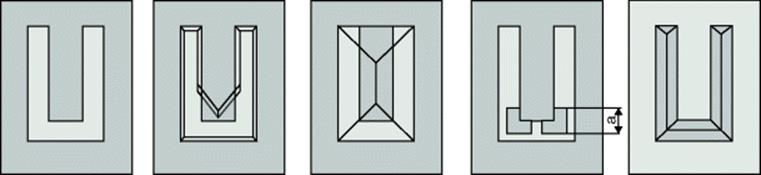
Waiting for the natural etch stop means that “L-,” “T-,” or “U”-shaped V-troughs necessary for microreactors cannot be produced. For these, etching is interrupted. The etching is interrupted when the desired depth has been reached. These V-cross-section troughs have convex 90° corners at any bends, and at those points, there is considerable undercutting of the mask. The remedy is corner compensation. Sacrificial surfaces are created at the convex corners, calculated in such a way that the etch time in the direction of the convex 90° corner will produce the correct shape.
Figure 3.10 shows the effect of various corner compensation arrangements. Corner compensation, if given the right dimensions, is capable of ensuring the production of channels in a variety of depths and even for etching right through the wafer. Cavities and holes can be achieved in one process. If a two-sided process is employed, V-troughs can be created on each side and these can even be connected by holes etched right through. Such structures with holes are required for connection positioned on top or to permit fluid connection between the individual layers. If channels with a trapezoid cross-section are needed, the depth of the channel is set by the etch time. See Refs [6–9] for more details.