CHEMISTRY THE CENTRAL SCIENCE
12 SOLIDS AND MODERN MATERIALS
12.7 COVALENT-NETWORK SOLIDS
Covalent-network solids consist of atoms held together in large networks by covalent bonds. Because covalent bonds are much stronger than intermolecular forces, these solids are much harder and have higher melting points than molecular solids. Diamond and graphite, two allotropes of carbon, are two of the most familiar covalent-network solids. Other examples are silicon, germanium, quartz (SiO2), silicon carbide (SiC), and boron nitride (BN).
In diamond, each carbon atom is bonded tetrahedrally to four other carbon atoms (![]() FIGURE 12.30). The structure of diamond can be derived from the zinc blende structure (Figure 12.27) if carbon atoms replace both the zinc and sulfide ions. The carbon atoms are sp3-hybridized and held together by strong carbon-carbon single covalent bonds. The strength and directionality of these bonds make diamond the hardest known material. For this reason, industrial-grade diamonds are employed in saw blades used for the most demanding cutting jobs. The stiff, interconnected bond network is also responsible for the fact that diamond is one of the best-known thermal conductors. Not surprisingly, diamond has a high melting point, 3550 °C.
FIGURE 12.30). The structure of diamond can be derived from the zinc blende structure (Figure 12.27) if carbon atoms replace both the zinc and sulfide ions. The carbon atoms are sp3-hybridized and held together by strong carbon-carbon single covalent bonds. The strength and directionality of these bonds make diamond the hardest known material. For this reason, industrial-grade diamonds are employed in saw blades used for the most demanding cutting jobs. The stiff, interconnected bond network is also responsible for the fact that diamond is one of the best-known thermal conductors. Not surprisingly, diamond has a high melting point, 3550 °C.
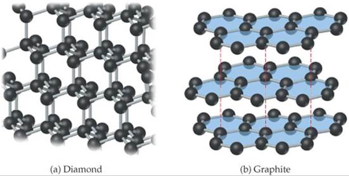
![]() FIGURE 12.30 The structures of (a) diamond and (b) graphite. The blue color in (b) is added to emphasize the planarity of the carbon layers.
FIGURE 12.30 The structures of (a) diamond and (b) graphite. The blue color in (b) is added to emphasize the planarity of the carbon layers.
In graphite (Figure 12.30b), the carbon atoms form covalently bonded layers that are held together by intermolecular forces. The layers in graphite are the same as the graphene sheet shown in Figure 12.8. Graphite has a hexagonal unit cell containing two layers offset so that the carbon atoms in a given layer sit over the middle of the hexagons of the layer below. Each carbon is covalently bonded to three other carbons in the same layer to form interconnected hexagonal rings. The distance between adjacent carbon atoms in the plane, 1.42 Å, is very close to the CC distance in benzene, 1.395 Å. In fact, the bonding resembles that of benzene, with delocalized π bonds extending over the layers. ![]() (Section 9.6) Electrons move freely through the delocalized orbitals, making graphite a good electrical conductor along the layers. (In fact, graphite is used as a conducting electrode in batteries.) These sp2-hybridized sheets of carbon atoms are separated by 3.35 Å from one another, and the sheets are held together only by dispersion forces. Thus, the layers readily slide past one another when rubbed, giving graphite a greasy feel. This tendency is enhanced when impurity atoms are trapped between the layers, as is typically the case in commercial forms of the material.
(Section 9.6) Electrons move freely through the delocalized orbitals, making graphite a good electrical conductor along the layers. (In fact, graphite is used as a conducting electrode in batteries.) These sp2-hybridized sheets of carbon atoms are separated by 3.35 Å from one another, and the sheets are held together only by dispersion forces. Thus, the layers readily slide past one another when rubbed, giving graphite a greasy feel. This tendency is enhanced when impurity atoms are trapped between the layers, as is typically the case in commercial forms of the material.
Graphite is used as a lubricant and as the “lead” in pencils. The enormous differences in physical properties of graphite and diamond—both of which are pure carbon—arise from differences in their three-dimensional structure and bonding.
Semiconductors
Silicon and germanium lie immediately below carbon in the periodic table. Like carbon, each of these elements has four valence electrons, just the right number to satisfy the octet rule by forming single covalent bonds with four neighbors. Hence, silicon and germanium, as well as the gray form of tin, crystallize with the same infinite network of covalent bonds as diamond.
When atomic s and p orbitals overlap, they form bonding molecular orbitals and antibonding molecular orbitals. Each pair of s orbitals overlaps to give one bonding and one antibonding molecular orbital, whereas the p orbitals overlap to give three bonding and three antibonding molecular orbitals. The extended network of bonds leads to the formation of the same type of bands we saw in discussing the electronic structures of metals in Section 12.4. The band that forms from bonding molecular orbitals is called the valence band, and the band that forms from antibonding orbitals is called the conduction band (![]() FIGURE 12.31). In a semiconductor, the valence band is filled with electrons and the conduction band is empty. These two bands are separated by an energy band gap, Eg.
FIGURE 12.31). In a semiconductor, the valence band is filled with electrons and the conduction band is empty. These two bands are separated by an energy band gap, Eg.
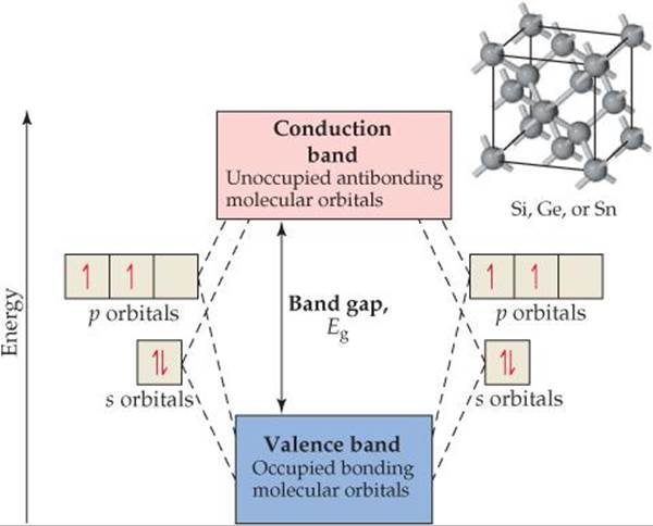
![]() FIGURE 12.31 The electronic band structure of semiconductors that have the diamond crystal structure.
FIGURE 12.31 The electronic band structure of semiconductors that have the diamond crystal structure.
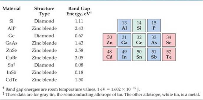
Semiconductors can be divided into two classes, elemental semiconductors, which contain only one type of atom, and compound semiconductors, which contain two or more elements. The elemental semiconductors all come from group 4A. As we move down the periodic table, bond distances increase, which decreases orbital overlap. This decrease in overlap reduces the difference between the bonding molecular orbitals of the valence band and the antibonding molecular orbitals of the conduction band. As a result, the band gap decreases on going from diamond (5.5 eV) to silicon (1.11 eV) to germanium (0.67 eV) to gray tin (0.08 eV). Moving one element down to lead, the band gap collapses altogether. As a result, lead has the structure and properties of a metal.
Note that in discussing semiconductors, the electron volt, eV, is the preferred energy unit: 1 eV = 1.602 × 10⁻¹⁹ J.*
Compound semiconductors maintain the same average valence electron count as elemental semiconductors—four per atom. For example, when gallium (group 3A) and arsenic (group 5A) combine to form gallium arsenide, GaAs, each Ga atom contributes three electrons and each As atom contributes five, which averages out to four per atom—the same number as in silicon or germanium. Hence, GaAs is a semiconductor. Other examples are InP, where indium contributes three valence electrons and phosphorus contributes five, and CdTe, where cadmium provides two valence electrons and tellurium contributes six. In both cases, the average is again four valence electrons per atom. GaAs, InP, and CdTe all crystallize with a zinc blende structure.
There is a tendency for the band gap of a compound semiconductor to increase as the difference in group numbers increases. For example, the band gap in a Ge semiconductor (made up of only group 4A atoms) is 0.67 eV, but the gap in a GaAs semiconductor (made up of 3A atoms and 5A atoms) is 1.43 eV. If we increase the difference in group number to four, as in ZnSe (groups 2B and 6A), the band gap increases to 2.70 eV. Increasing the horizontal separation of the elements even more leads to a band gap of 3.05 eV in CuBr. This progression is a result of the transition from pure co-valent bonding in elemental semiconductors to polar covalent bonding in compound semiconductors. As the difference in electronegativity of the elements increases, the bonding becomes more polar and the band gap increases.
Electrical engineers manipulate both the orbital overlap and the bond polarity to control the band gaps of compound semiconductors for use in a wide range of electrical and optical devices. The band gaps of several elemental and compound semiconductors are given in ![]() TABLE 12.4.
TABLE 12.4.
TABLE 12.4 • Band Gaps of Select Elemental and Compound Semiconductors
SAMPLE EXERCISE 12.3 Qualitative Comparison of Semiconductor Band Gaps
Will GaP have a larger or smaller band gap than ZnS? Will it have a larger or smaller band gap than GaN?
SOLUTION
Analyze The size of the band gap depends on the vertical and horizontal positions of the elements in the periodic table. The band gap will increase when either of the following conditions is met: (1) The elements are located higher up in the periodic table, where enhanced orbital overlap leads to a larger splitting between bonding and antibonding orbitals, or (2) the horizontal separation between the elements increases, which leads to an increase in the electronegativity difference and bond polarity.
Plan We must look at the periodic table and compare the relative positions of the elements in each case.
Solve Gallium is in the fourth period and group 3A. Phosphorus is in the third period and group 5A. Zinc and sulfur are in the same periods as gallium and phosphorus, respectively. However, zinc, in group 2B, is one element to the left of gallium; sulfur in group 6A is one element to the right of phosphorus. Thus, we would expect the electronegativity difference to be larger for ZnS, which should result in ZnS having a larger band gap than GaP.
For both GaP and GaN the more electropositive element is gallium. So we need only compare the positions of the more electronegative elements, P and N. Nitrogen is located above phosphorus in group 5A. Therefore, based on increased orbital overlap, we would expect GaN to have a larger band gap than GaP.
Check External references show that the band gap of GaP is 2.26 eV, ZnS is 3.6 eV, and GaN is 3.4 eV.
PRACTICE EXERCISE
Will ZnSe have a larger or smaller band gap than ZnS?
Answer: Because zinc is common to both compounds and selenium is below sulfur in the periodic table, the band gap of ZnSe will be smaller than ZnS.
Semiconductor Doping
The electrical conductivity of a semiconductor is influenced by the presence of small numbers of impurity atoms. The process of adding controlled amounts of impurity atoms to a material is known as doping. Consider what happens when a few phosphorus atoms (known as dopants) replace silicon atoms in a silicon crystal. In pure Si all of the valence-band molecular orbitals are filled and all of the conduction-band molecular orbitals are empty as ![]() FIGURE 12.32 (a) shows. Because phosphorus has five valence electrons but silicon has only four, the “extra” electrons that come with the dopant phosphorus atoms are forced to occupy the conduction band [Figure 12.32(b)]. The doped material is called an n-type semiconductor, n signifying that the number of negatively charged electrons in the conduction band has increased. These extra electrons can move very easily in the conduction band. Thus, just a few parts per million (ppm) of phosphorus in silicon can increase silicon's intrinsic conductivity by a factor of a million!
FIGURE 12.32 (a) shows. Because phosphorus has five valence electrons but silicon has only four, the “extra” electrons that come with the dopant phosphorus atoms are forced to occupy the conduction band [Figure 12.32(b)]. The doped material is called an n-type semiconductor, n signifying that the number of negatively charged electrons in the conduction band has increased. These extra electrons can move very easily in the conduction band. Thus, just a few parts per million (ppm) of phosphorus in silicon can increase silicon's intrinsic conductivity by a factor of a million!
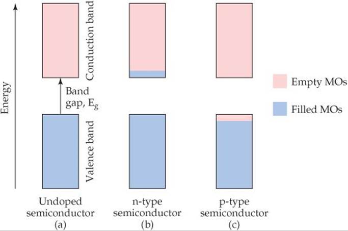
![]() FIGURE 12.32 The addition of small amounts of impurities (doping) to a semiconductor changes the electronic properties of the material.
FIGURE 12.32 The addition of small amounts of impurities (doping) to a semiconductor changes the electronic properties of the material.
The dramatic change in conductivity in response to the addition of a trace amount of a dopant means that extreme care must be taken to control the impurities in semiconductors. It also provides an opportunity for controlling the electrical conductivity through precise control of the type and concentration of dopants.
It is also possible to dope semiconductors with atoms that have fewer valence electrons than the host material. Consider what happens when a few aluminum atoms replace silicon atoms in a silicon crystal. Aluminum has only three valence electrons compared to silicon's four. Thus, there are electron vacancies, known as holes, in the valence band when silicon is doped with aluminum [Figure 12.32(c)]. Since the negatively charged electron is not there, the hole can be thought of as having a positive charge. Any adjacent electron that jumps into the hole leaves behind a new hole. Thus, the positive hole moves about in the lattice like a particle.* A material like this is called a p-type semiconductor, p signifying that the number of positive holes in the material has increased.
As with n-type conductivity, p-type dopant levels of only parts per million can lead to a millionfold increase in conductivity—but in this case, the holes in the valence band are doing the conduction [Figure 12.32(c)].
The junction of an n-type semiconductor with a p-type semiconductor forms the basis for diodes, transistors, solar cells, and other devices.
SAMPLE EXERCISE 12.4 Identifying Types of Semiconductors
Which of the following elements, if doped into silicon, would yield an n-type semiconductor: Ga, As, or C?
SOLUTION
Analyze An n-type semiconductor means that the dopant atoms must have more valence electrons than the host material. Silicon is the host material in this case.
Plan We must look at the periodic table and determine the number of valence electrons associated with Si, Ga, As, and C. The elements with more valence electrons than silicon are the ones that will produce an n-type material upon doping.
Solve Si is in column 4A, and so has four valence electrons. Ga is in column 3A, and so has three valence electrons. As is in column 5A, and so has five valence electrons; C is in column 4A, and so has four valence electrons. Therefore, As, if doped into silicon, would yield an n-type semiconductor.
PRACTICE EXERCISE
Suggest an element that could be used to dope silicon to yield a p-type material.
Answer: Because Si is in group 4A, we need to pick an element in group 3A. Boron and aluminum are both good choices—both are in group 3A. In the semiconductor industry boron and aluminum are commonly used dopants for silicon.