Microreactors in Organic Chemistry and Catalysis, Second Edition (2013)
3. Microreactors Made of Glass and Silicon
3.3. Isotropic Wet Chemical Etching of Silicon
Isotropic etching of silicon is done with an aqueous mixture of HF + HNO3 + CH3COOH (hydrofluoric, nitric acid, and acetic acid). Often, the acetic acid is omitted. The etch rates are very high at room temperature: 940 μm/min with 20–46% HNO3 (69% HNO3, 31% H2O) complemented by HF (49% HF, 51% H2O). The quality of the silicon surface produced will depend on the solution used. Smoother surfaces are achieved with a higher proportion of nitric acid and a lower proportion of acetic acid.
The disadvantage is the low degree of selectivity as a far as silica is concerned. For SiO2, the etch rates are between 300 and 700 nm/min. Silicon nitride and noble metals demonstrate better resistance to etching. Because of the isotropy, the aspect ratio is only 0.5. Therefore, it is very seldom employed for the creation of structures to be used in microreactors [2].
3.3.1.1 Isotropic Wet Chemical Etching of Silicon
In contrast to anisotropic wet etching, reactive dry etching offers the possibility of creating a relatively free selection of geometric patterns independent of the crystal orientation. For the use here being described, the most suitable method is reactive ion etching, RIE. RIE is a combination of etching by sputtering (a purely physical method) and plasma etching (a purely chemical method). It makes simultaneous use of energetic particles and reactive plasma particles to remove material. The apparatus used is the same as that for sputter etching, Figure 3.11. The main difference from sputtering alone is that instead of the inert gas, a reactive gas (or mixture containing one) is fed into the reactor. The energetic particles always knock out surface particles with a sputter effect, whether or not there is chemical reaction. But, RIE means there is also a chemical reaction between the reactive gas and the substrate: in this, RIE is like plasma etching. The unwanted material is removed physically, but there is assistance from some chemical reaction at the surface [6]. The physical part of the process is anisotropic and the chemical isotropic. Different etching profiles can be set by judicious selection of parameters, Figure 3.12.
Figure 3.11 Apparatus for RIE.
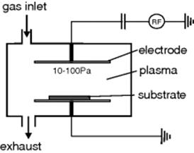
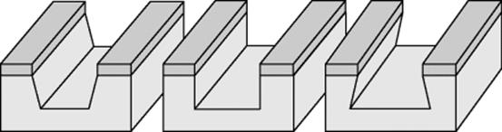
Figure 3.12 Different etching profiles, set up by selection of parameters.
Various procedures are used. One common dry chemical etching process employed in microreactor manufacture is deep reactive ion etching, DRIE. To increase the anisotropy, the RIE procedure is modified so that as the etching advances, some of the reaction products settle on the sidewall passivating it. Reaction products at the front to which the etch has advanced are removed by means of physical components. The resulting troughs are very deep, with vertical walls. The etch rate will depend on the pattern left open by the mask and on the depth to which etching is permitted. Troughs of different widths will etch to different depths in the same period of time [6, 10, 11]
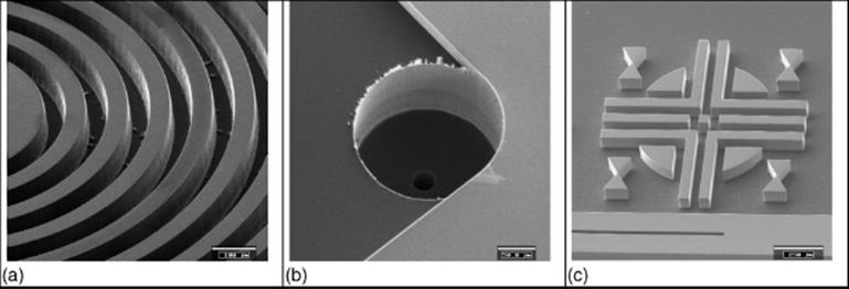
The gas mixture used to etch the silicon consists of SF6 and O2; SF6+ ions and oxygen radicals are generated in the plasma. Photoresist is the masking layer employed in DRIE. Aspect ratios up to 50 are possible. The channels can be formed on any pattern and will have a rectangular cross-section. A two-sided process or two-stage masking is used if holes are required in combination with cavities. The Figure 3.13 shows examples.
Figure 3.13 Examples of RIE-etched silicon. (a) Circular channels, (b) channel with a through-hole, and (c) adjustment mark. Source: With courtesy of the Technical University of Ilmenau, Faculty of Mechanical Engineering, Department of Micromechanical Systems.
3.3.1.2 Isotropic Wet Chemical Etching of Silicon Glass
In the case of glass, which has higher chemical resistance than does silicon, the choice of structuring procedures is narrower for this reason. One possibility is isotropic wet chemical etching (Figure 3.14). The nature of the process means the aspect ratio is only 0.5. The choices of masking material are polysilicon, chromium–nickel, or chromium–gold; for the application of the mask and the structuring, see Table 3.3. The structuring of the layer depends on lithography. As the masking layer is applied, defects, known as pinholes, may develop. Depending on the window in the manufacturing process, the number of pinholes may vary in the particular procedure. As the etching is isotropic, mask defects are magnified. The tiniest gap will lead to a hole with a diameter twice the depth of the etch. Layer combinations are often used as a way to prevent pinholes.
Figure 3.14 Isotropic wet chemical etching of silicon glass (with friendly permission of the Institute of Physical High Technology).
Whenever there is chemical erosion of glass, water or its dissociation products, H+ or OH− ions, will be involved. Because of this, a distinction is made between the resistance of glass to water (its hydrolytic resistance) and to alkali or acid. Under attack from water or acids, small numbers of cations, particularly monovalent and divalent, are released. On resistant types of glass, a very thin layer of silica gel forms in this way on the glass surface and usually inhibits further erosion. In contrast, hydrofluoric acid, alkaline solutions, and, under certain circumstances, phosphoric acid will slowly remove the inhibitor layer and thus the entire surface. Nonaqueous solutions (organic solutions), however, are practically nonreactive with glass.
The pinhole problem, adhesion difficulty, and low aspect ratio all restrict the depth of the etch for the structuring. Depths down to 120 μm are achieved simply; in Ref. [12], there is a report of 300 μm achieved by using a 1 μm Cr/Au masking system.
Through-holes are only possible in very thin substrates. This process can be combined with other means of structuring glass: for example, microsandblasting or ultrasonic lapping.
3.3.2 Other Processes
3.3.2.1 Photostructuring of Special Glass
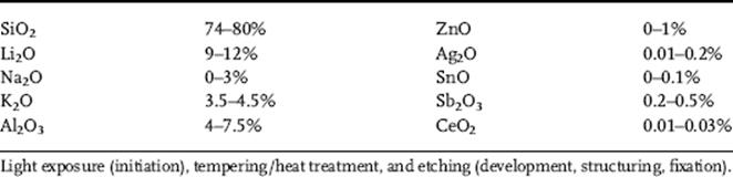
None of the etching processes described so far enables structures to be created in glass, which have a high aspect ratio or which have the cross-sections necessary for microreactors. To allow the manufacture of fine structures with a high aspect ratio in glass, a number of photostructurable types of glass have been developed in parallel. These types are based on the general threefold glass system, Li2O-Al2O3-SiO2, with tiny amounts of additive, making them photosensitive. A photolithographic process imparts a structure to these types of glass, following procedures similar to that with photoresists. In Table 3.4, the approximate composition of photostructurable types of glass is given.
Table 3.4 Configuration of photostructurable special glass.
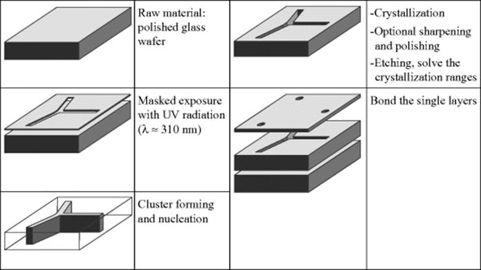
The process followed with glass is more complicated than shown below, but the description is adequate to an understanding of the sequence. The glass is melted under reducing conditions so that cerium is present in the form of Ce3+ and silver in the form of Ag+. The Ce3+ will emit another electron if illuminated with UV light (λ = 300–320 nm), and this electron can be taken up by the Ag+ to form Ag0. The amount of energy required for complete illumination will depend on the thickness of the glass. If the illumination is insufficient, the substrate is not illuminated right through.
Heat treatment brings the silver atoms together into clusters that are then nuclei for the lithium metal silicate crystals. The heat treatment has two critical thermal points, 1 h at ~500 °C during which time the silver clusters group, and another hour at 600 °C. The lithium metal silicate crystals are generated at the higher temperature. The size of these crystals is between 1 and 10 μm, depending on the temperature profile employed and to the composition of the glass. The lithium metal silicate crystals are 10–60 times more soluble in dilute hydrofluoric acid as the glass would be if not illuminated. It is then possible to selectively dissolve the areas that have been exposed to light and become crystalline. Reinforcement with ultrasound is useful in order to remove remnants of glass from the edges of the crystallized areas. The following illustrations, Figure 3.15, show samples of structures
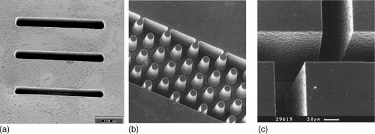
Figure 3.15 Examples of structures in photostructuring glass (a) long hole, (b) columns, and (c) interlocking channels. Source: With courtesy of the Technical University of Ilmenau, Faculty of Mechanical Engineering, Department of Inorganic-Nonmetallic Materials.
When a reactor is being manufactured, both, cavities and through-holes, are required. In the case of photosensitive glass, it is difficult to make troughs. The necessary illumination goes right through the wafer, and so, there are crystallized areas going right through and these are then dissolved out. Cavities and islands are thus impossible to create in this manner. The following illustrations, Figure 3.16, show the basic steps. For the manufacture of islands, a wafer that has not been completely etched through is necessary, or else the islands will drop out. It is possible to create them by interrupting the etching: once the necessary depth has been reached, the etching process is stopped. However, this is not very desirable, as the wafer will now consist of crystallized areas and of glass, two components with different thermal and chemical properties. Ref. [12] gives a description of all the other procedures using gray scale masking and multiple exposures. Reactors are virtually monolithic, made completely out of the same material. It is thus only in exceptional cases that the manufacturing procedure includes interrupted etching.
Figure 3.16 Basic steps for the photostructuring of glass: Light exposure (initiation), tempering/heat treatment and etching (development, structuring, fixation).
The crystal phase and the surrounding glass have different coefficients of thermal expansion and different densities. The heat treatment and attendant critical transformation temperature cause distortion and some slight bulging of the wafer, which makes subsequent joining procedures more difficult. Once it has been etched, the wafer bares delicate open structures and cannot mechanically be processed further. If the wafer is polished before it is etched, the bulging can be counteracted, so that even after etching, it is more or less flat. Examples of structures are shown in Figure 3.15, see Refs [13–17] for more details.
3.3.3 Drilling, Diamond Lapping, Ultrasonic Lapping
As is described in more detail in Section 1.2.2, glass is so hard that it is mainly processed by machining using cutter mechanisms with indefinite geometry, such as ultrasound lapping (and, in older systems, ultrasound drilling). High-frequency electrical energy is converted by a piezo-ceramic sound converter into mechanical vibration at the same frequency. The amplitude of the longitudinal vibration of the sound converter is only 5 μm. For this reason, another unit is set between the shaping tool and the sound converter. This consists of an amplitude transformer and a sonotrode (also known as drill), which amplifies the value to between 20 and 40 μm.
The four elements connected together are a vibratory system operating in resonance with each other. The system permits a process based on the hammering of the grains into the surface of the tool within the ultrasound range (19–22 kHz), which creates tiny cracks and eventually detaches small fragments. This process mainly takes place in the direction of movement of the ultrasound vibration. If possible, the use of rotating tools is advised, as they achieve better removal. The grains are contained in a liquid or paste, the lapping medium. This mixture is either poured or pressed continuously into the gap between shaping tool and worked item. This gap should be approximately twice as wide as the average grain size. The choice of grain material usually falls on boron carbide because of its fracture capability and consequent self-sharpening. The boron carbide constitutes about 25–35% of the mass of the lapping medium and is usually in grain size 50–60 μm. As the tool is under the same strain as the worked item, it must be made of a material that is either harder or does at least have adequate resistance to abrasion. For that reason, steels are usually used as they tend to be deformed elastically and plastically by the impact of the grains. The main area in which ultrasound lapping is used for microreactor manufacture is in the drilling of external or internal connecting holes such as holes in glass lids used to seal fine structures made of silicon or glass.
3.3.4 Micro Powder Blasting
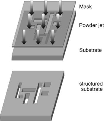
Microabrasion using compressed air is a modification based on sand blasting, the micro powder blasting. This process enables all types of glass, ceramics, and semiconductor materials, whatever their chemical composition and crystal structure to be inexpensively processed down to the micrometer scale. The micro powder blasting is a masked procedure; it works quasi parallel on the whole substrate. A powder jet drives systematically, over the substrate. Material is removed at the mask openings (Figure 3.17).
Figure 3.17 Principle of masked microabrasives powder blasting.
The depth of structure achieved will depend on the processing time. The aspect ratio is 2–3, and the smallest structure that can be created is 50 μm. The masks are created with photolithography. The process permits both very fine tolerances of shape and position and also allows as many lateral structures/side by side as desired, densely packed. The mechanical nature of the procedure means that the chemical composition of the material is unimportant. As the items are not exposed to heat, there is no distortion. One disadvantage is the angle of the abraded contours to the surface of the substrate. It will be 70° to 85°, depending on the depth sought. Deeper structures have steeper sides. Figure 3.18 shows different structuring processes. The depth of the structures is determined with the operating time. It is possible single and double-sided processing. By a repeated masking, structures can be realized as in Figure 3.18c, with cavities and through-holes on both sides. The tolerances and surface quality for this procedure are similar to those of ultrasonic drilling/lapping.
Figure 3.18 Example structures.
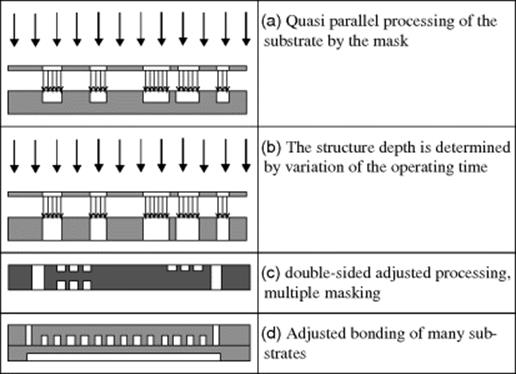
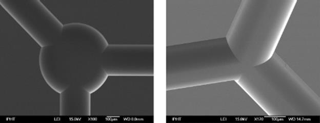
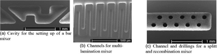
Figure 3.19 gives examples of structures achieved by microabrasion. Cavities and breakthroughs are possible, either using a single-side or a double-side procedure.
Figure 3.19 Manufactured structures by sandblasting for micromixers. Source: With courtesy of the Little Things Factory GmbH, Ilmenau, Germany.
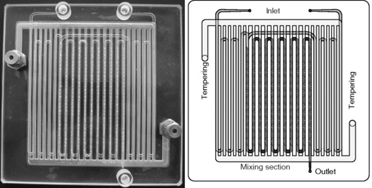
The roughness of the finished surface is Rz ≈ 2–4 μm. Surfaces treated by lapping and microabrasion are similar. In contrast to what happens to photostructured glass, only the areas without a mask are in anyway processed; the covered parts of the wafer surface remain virtually intact. Figure 3.20 shows various examples of one-sided and double-sided structuring.
Figure 3.20 Example of microreactors (150 mm × 150 mm), with two functional layers: outside: tempering, inside: preliminary heating, mixing, dwell channel (volumes ~3 ml). Source: With courtesy of the Little Things Factory GmbH, Ilmenau, Germany [18–24].
The ideal process can be selected for a particular application if one knows the nature of various procedures. It is also possible to combine procedures.
3.3.5 Summary
The difficulties of processing glass have already been described. The following are the other technologically significant methods.