Microreactors in Organic Chemistry and Catalysis, Second Edition (2013)
2. Fabrication of Microreactors Made from Metals and Ceramic
2.2. Etching
From silicon and other semiconductor technologies, dry and wet etching techniques are well known. For many metals, etching is a relatively cheap and well-established technology to obtain freeform structures with dimensions in the submillimeter range. The technology is well described in the literature [1–5, 9]. A photosensitive polymer mask material is applied onto the metal to be etched. The mask is exposed to light via a structure primary mask. Here, different technologies are used, details of which can be found in the literature for semiconductor processing or in Refs [1–3]. Then, the polymer is developed. This means the nonexposed parts are polymerized in such a way that they are not diluted by the solvent used to remove the rest of the polymer covering the parts to be etched. Thus, a mask is formed, and the metal is etched through the openings of this mask. To generate the etching mask, other techniques such as direct mask writing with a laser are also used commonly.
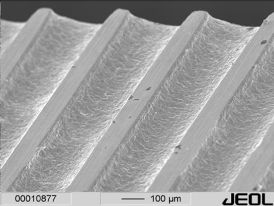
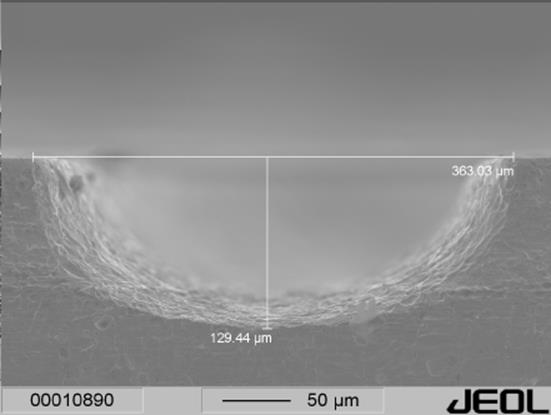
When etching techniques are used, two main considerations have to be taken into account. First, the aspect ratio (the ratio between structure width and structure depth) can, for wet chemical etching, only be <0.5 at the optimum. Due to the isotropic etching of the wet solvents, the minimum width of a structure is two times the depth plus the width of the mask openings. Dry etching (e.g., laser) is not limited to this aspect ratio, but shows other limitations and is rather expensive (see Ref. [1]). Second, wet chemical etching always results in semielliptic or semicircular structures, again due to the isotropic etching. Dry etching often leads to other channel geometries. Here, rectangular channels are possible. In Figure 2.1, a stainless steel microchannel structure manufactured by wet chemical etching is shown. The microchannels are used to build a chemical reactor for heterogeneously catalyzed gas-phase reactions. They are about 360 μm wide and 130 μm deep. Figure 2.2 shows the details of the entrance area of such a microchannel. The semicircular structure is clearly seen. Details of the etching processes and etching agents can be found in Refs [1, 4, 9, 10].
Figure 2.1 Wet chemically etched microchannels in a stainless steel foil.

Figure 2.2 Details of the microchannels from Figure 2.1. Clearly, the semielliptic shape of the channels is shown. The microchannel is about 360 μm wide and 130 μm deep.
