Physical Chemistry Essentials - Hofmann A. 2018
Catalysis
7.3 Methods to Investigate Surfaces and Surface Processes
In heterogeneous catalysis, catalysis happens on the surface of the catalyst (also called adsorbent or substrate). Therefore, in order to investigate processes at surfaces, or indeed their make-up, experimental techniques are required. Two types of methods of surface investigation can be distinguished: spectroscopic methods and imaging methods.
The choice of a particular spectroscopic method depends on what exactly is to be investigated. From Fig. 7.11, which shows the electromagnetic spectrum, it is obvious that different energy regions of the spectrum need to be employed, depending on whether bonds between adsorbate and substrate molecules are to be investigated, or atomic information is required. A frequent problem in practical applications is, for example, the chemical composition of a surface. This can be determined by using ionising electromagnetic radiation such as X-rays (see also Sect. 13.5) or hard UV. The interaction of a beam of high energy electromagnetic radiation leads to a variety of effects in a solid sample (Fig. 7.12) which can be used to characterise the specimen.
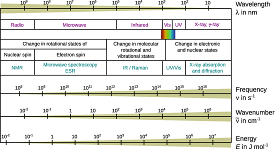
Fig. 7.11
The electromagnetic spectrum
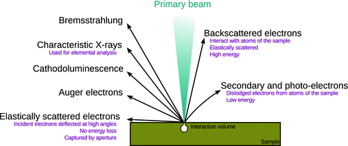
Fig. 7.12
Interaction of a beam of high energy electromagnetic radiation with a solid specimen
Whereas spectroscopic methods result in ’abstract’ information about a sample, imaging methods provide pictures as to the distribution of features or physical structures of samples and typically yield ’images’ as an immediate result of the experiment. In the following, a few methods used in surface characterisation will be briefly introduced.
7.3.1 Photoelectron Spectroscopy
This method is based on the photoelectric effect which was originally observed by James Franck and Gustav Hertz, and later explained by Albert Einstein. Light of sufficiently high energy can be used to ionise a sample, giving rise to photo electrons from species present. Depending on whether X-rays or hard UV radiation is used, the method is called XPS or UPS (see also Sect. 13.5.1). Since the kinetic energy of electrons ejected from an atom depends on the internal electronic structure of that atom, information about the electronic structure and chemical composition is obtained (Fig. 7.13).
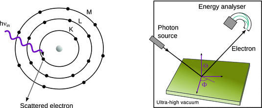
Fig. 7.13
Schematic illustration of the photoelectric effect (left) and its application in photoelectron spectroscopy
7.3.2 Auger Electron Spectroscopy
The Auger effect is the emission of an electron after incident high energy caused loss of an electron. The hole left by the first departing electron is filled by a second electron from a higher shell that takes the place of the first electron. This transition releases energy which can either be emitted as a photon (X-ray fluorescence; see Sect. 7.3.3) or lead to ejection of a third electron, called the Auger electron (see Fig. 7.14). The energies of the Auger electrons are characteristic of the species present which makes Auger electron spectroscopy a useful tool for determination of the chemical identities in samples. The incident energy may be provided by X-ray, hard UV or electron beams. The Auger process is discussed in more detail in Sect. 13.6.3.
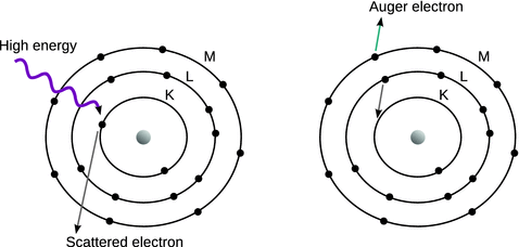
Fig. 7.14
Schematic illustration of the Auger effect
7.3.3 X-ray Fluorescence
Arising from the same physical process as the Auger electrons, photons may be emitted instead of secondary electrons (Fig. 7.15, left panel). In this case, the process is called X-ray fluorescence (see also Sect. 13.6.2). Again, spectral analysis of the emitted energies allows conclusions as to the species present. By rastering a sample through the incoming beam of high energy photons and determining the energy of the emitted X-rays, a spatial mapping can be performed (Fig. 7.15, right panel). In doing so, the spectroscopic method of X-ray fluorescence becomes an imaging method and is thus called X-ray fluorescence microscopy.
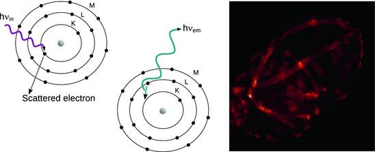
Fig. 7.15
Left: The emission of a photon instead of an Auger electron (after electron loss due to high energy impact) is called X-ray fluorescence. Right: An X-ray fluorescence micrograph mapping iron in the egg of the parasitic worm Schistosoma japonicum. Figure adapted from Hofmann et al. (2014)
7.3.4 LEED
The arrangement of atoms close to the surface can be determined by low energy electron diffraction ( LEED). Here, the wave character of electrons is used. An incident electron beam of relatively low energy (typically in the range 20—200 eV) is diffracted by the atomic lattice formed by atoms on or close to the surface. The diffracted electrons can be observed by a fluorescent screen, and the resulting diffraction pattern is then visible from behind the sample (modern instruments use a position sensitive detector instead of the fluorescent screen, thus enabling digital data acquisition). The diffraction pattern represents the two-dimensional reciprocal lattice of the specimen’s surface.
As introduced in Sect. 7.2.1, hardly any surface is an ideal surface (i.e. like a cut through the bulk material). Instead, there are many terraces, steps and kinks in surfaces of solids which can be identified with LEED. Besides characterisation of the basic lattice of a solid sample, further information can be gained from particular features caused by super lattices, step lattices or domain formation (Fig. 7.16).
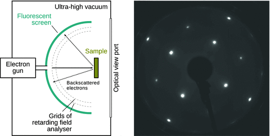
Fig. 7.16
Left: Schematics of a LEED instrument. The concentric grids are used for filtering inelastically scattered electrons. Instead of optical observation of the LEED pattern, modern instruments have a position-sensitive digital detector (called delay-line detector) instead of the fluorescent screen. Right: LEED pattern of an Ir(100)−1 × 1 surface recorded at an energy of 195 eV. The image was kindly provided by L Hammer (Friedrich-Alexander-Universität Erlangen-Nürnberg, Germany) and is reproduced with permission
Like photo-electron and Auger electron spectroscopy, LEED requires the sample to be brought into an chamber of ultra high vacuum. The correct alignment of the crystalline sample can be achieved with the help of X-ray diffraction. After mounting, the specimen is cleaned chemically by oxidation/reduction cycles and the surface flattened using exposure to high temperature. This process (called annealing) may lead to re-surfacing of impurities. Therefore, Auger electron spectroscopy is often used in conjunction with LEED to monitor the purity of the sample.
7.3.5 Scanning Probe Methods
Most of the surface methods mentioned in the previous sections deliver information about the surface of materials from which information about topological features is available by means of reconstruction. However, we have also seen that X-ray fluorescence can be used in conjunction with raster scanning of the sample, thus directly resulting in an image.
Scanning probe methods are based on a similar principle; here, a probe is raster scanning over a surface, and the interaction between the probe and the surface is measured. The most scanning probe methods are scanning tunneling microscopy and atomic force microscopy (AFM). In both cases, the physical elevation of surfaces (z-direction) is probed.
Scanning Tunneling Microscopy (STM)
Gerd Binnig and Heinrich Röhrer (Nobel prize in 1986) developed STM in the early 1980s. A sharp metal tip is brought into a distance of 2—5 Å of a conducting surface, and a potential of about 2 V is applied between the tip and the sample. In this configuration, electrons can tunnel across the gap between the tip and the sample, and the current depends on the distance between the tip and surface in an exponential fashion. This strong dependence is the reason for the high resolving power of STM which allows imaging an true atomic resolution.
Atomic Force Microscopy ( AFM)
This surface-sensitive method enables imaging of surfaces or detection of interactions between molecules; it was conceived by Binnig and colleagues in the mid-1980s as a further development of STM. In AFM, the surface is visualised in three dimensions by touching it with a tiny probe called the tip. The physical phenomenon probing surface elevation is the interaction force between the tip and the sample surface.
Attractive or repulsive forces between tip and surface are observed through measurement of the reflection of a laser beam by the cantilever. The reflected laser beam is detected by a photodiode detector which converts the optical into an electrical signal. The microscope uses a feedback loop which triggers a z-movement of the piezoelectric scanner upon bending of the cantilever. The parameters of the feedback loop are optimised such as to minimise and maintain a constant value of the force between the tip and the sample.
The surface area (x- and y-direction) is scanned in a raster-like fashion with a tip brought very close to the sample. The tip is attached to the free end of a cantilever (Fig. 7.17) which will be bent due to interactions between the tip and the sample surface. It provides an image of the surface topography of the specimen at high resolution.
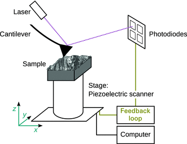
Fig. 7.17
Schematic illustration of an atomic force microscope. Figure kindly provided by A Simon (Université Lyon 1, France) and adapted from Hofmann et al. (2014)
The lateral resolution depends on the diameter and geometry of the tip apex. With conventional instruments, high resolution images at a lateral resolution of 0.5—1 nm (= 5—10 Å) can be obtained. The vertical resolution is higher, but limited by mechanical vibrations and thermal fluctuations of the cantilever. Typically, vertical resolutions of about 0.1—0.2 nm (= 1—2 Å) can be achieved. Further developments of this technique even allows imaging and characterisation of surfaces at subatomic resolution (Sugimoto et al. 2007; Emmrich et al. 2015) whereby single adatoms appear as toroidal structures and multi-atom clusters as connected structures, showing each individual atom as a torus (Fig. 7.18).
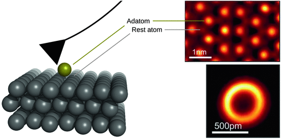
Fig. 7.18
AFM at sub-nanometer scale can visualise individual atoms. Right top: AFM image of the Si(111)-(7 × 7) reconstruction using a CO-terminated metal tip. The rest atoms and adatoms are clearly visible. Right bottom: AFM image of a Cu adatom on Cu(111), showing a ringlike symmetry that is caused by a toroidal charge density of the adatoms. Experimental AFM images are reproduced from Emmrich et al. (2015) with permission (License No 3691111422111)
AFM is a technique with a wide variety of applicability. It can operate in vacuum, air or liquid and be used to probe conductor or non-conductor surfaces. It can also be used with biological samples (see Fig. 7.19) and has become very popular in many fields, including materials science, polymer science, physics, life sciences and nano-biotechnology.
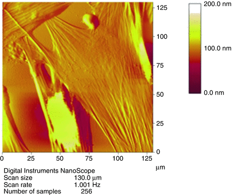
Fig. 7.19
Example of a biological AFM application: an AFM profile of cells (Simon et al. 2003) with a colour gradient indicating the vertical height. Figure kindly provided by A Simon (Université Lyon 1, France)